


The basic composition of PCB
o-leading.com
o-leading.com
2017-07-04 21:40:03
The current circuit board consists mainly of the following:
Line and surface (Pattern): the circuit is used as the tool between the original, and in the design, another large copper surface will be designed as the grounding and power supply layer. The lines and planes are made simultaneously.
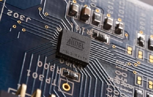
Dielectric layer (Dielectric): used to maintain insulation between lines and layers, commonly known as substrate.
The hole (Through hole / via): via the two levels above the line mutual conduction, large holes is used in parts, non conducting hole (nPTH) is usually used as a surface mount assembly with screw positioning.
Soldermasks (Solder resistant /Solder Mask): copper surface is not all to eat tin parts, so the non tin area, will be printed with a layer of insulation material copper tin (usually epoxy resin), avoid non tin line short circuit. According to different process, divided into green, blue, Chili oil oil.
Screen (Legend /Marking/Silk screen): This is a non essential component, the main function is to mark the parts on the circuit board name, location box, easy to assemble after maintenance and identification.
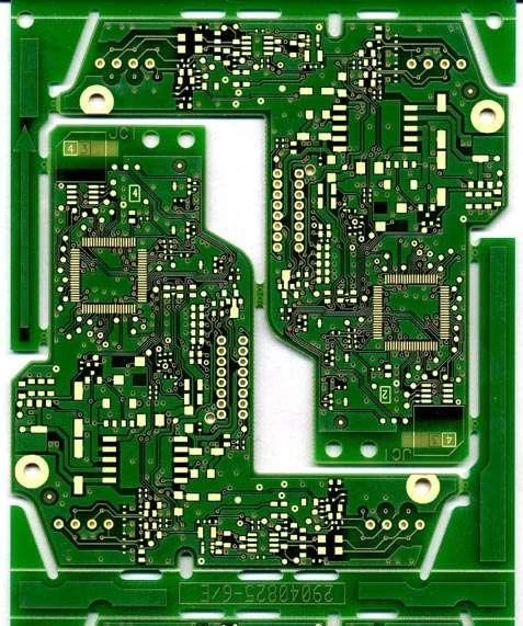
Surface (Finish): because the copper surface is easy to oxidize in the general environment, which leads to tin (solderability is not good), it will be protected on the copper surface where tin is eaten. The protection methods include tin (HASL), gold (ENIG), silver (Immersion, Silver), tin (Immersion, Tin), organic solder (OSP), each has its advantages and disadvantages, collectively referred to as surface treatment.
If you need, click this: Pcb design in china, pcb manufacturer in china, Small volume pcb manufacturer
Line and surface (Pattern): the circuit is used as the tool between the original, and in the design, another large copper surface will be designed as the grounding and power supply layer. The lines and planes are made simultaneously.
Dielectric layer (Dielectric): used to maintain insulation between lines and layers, commonly known as substrate.
The hole (Through hole / via): via the two levels above the line mutual conduction, large holes is used in parts, non conducting hole (nPTH) is usually used as a surface mount assembly with screw positioning.
Soldermasks (Solder resistant /Solder Mask): copper surface is not all to eat tin parts, so the non tin area, will be printed with a layer of insulation material copper tin (usually epoxy resin), avoid non tin line short circuit. According to different process, divided into green, blue, Chili oil oil.
Screen (Legend /Marking/Silk screen): This is a non essential component, the main function is to mark the parts on the circuit board name, location box, easy to assemble after maintenance and identification.
Surface (Finish): because the copper surface is easy to oxidize in the general environment, which leads to tin (solderability is not good), it will be protected on the copper surface where tin is eaten. The protection methods include tin (HASL), gold (ENIG), silver (Immersion, Silver), tin (Immersion, Tin), organic solder (OSP), each has its advantages and disadvantages, collectively referred to as surface treatment.
If you need, click this: Pcb design in china, pcb manufacturer in china, Small volume pcb manufacturer